
Empowering Next-Gen Smartphones: High-Density HDI FPC and Dynamic Flex Solutions for Mobile Innovation
The smartphone industry is advancing at breakneck speed, driven by foldable displays, multi-camera matrix modules, and 5G high-frequency communications. To pack cutting-edge capabilities into ultra-slim, compact chassis, hardware architects are replacing restrictive wiring layouts with advancedFlexible Printed Circuits (FPC).
As a leading B2B manufacturing partner, we specialize in delivering premium-gradeHDI FPCandMulti-layer FPCSolutions designed to unlock the full potential of next-generation mobile devices.
I. Seamless Integration for Foldable Displays and Premium Modules
Modern mobile architectures require components that can bend, fold, and twist without compromising signal integrity. Our custom-engineered circuits are designed to meet the most demanding spatial challenges inside today's flagship smartphones:
Foldable Display Modules:Engineered for high performanceDynamic Flexible FPCs, our designs deliver an ultra-tightBend Radiusand an extraordinaryFlex Cycle Life, ensuring flawless performance across hundreds of thousands of folds without trace cracking.
Compact Camera and Display Modules:Using ultra-fineTrace Width/Spaceand space-savingMicrovias, ourHDI FPCThe designs link high-resolution image sensors and OLED drivers with zero latency, maximizing space efficiency in crowded component areas.
Motherboard Interconnects:Replacing rigid boards with dual-sided and multi-layer flexible circuits enables smooth, multi-dimensional 3D routing across hinges and around tight internal boundaries.
II. Advanced Materials and Precision Impedance Control
To protect high-speed data transmission—including MIPI, PCIe, and 5G RF signals—we combine premium materials with rigorous electromagnetic engineering:
High-Tier Base Materials:We use premiumPolyimide (PI), Adhesive-free CCL, and low-lossLiquid Crystal Polymer (LCP)to maintain minimal insertion loss and exceptional thermal stability under heavy processing loads.
RA Copper Foil:We offer premium plansRolled Annealed (RA) Copperfor dynamic flexing areas to completely eliminate the risk of bending fatigue and micro-fractures.
Flawless Signal Integrity:Every high-speed differential trace is simulated using industry-standard field solvers (aligned with Polar Si9000 models) to clampCharacteristic Impedancetolerances tightly within a±5%golden window, completely eliminating "signal black holes".
III. World-Class Metallization and Zero-Defect Manufacturing
Reliability hinges on the micro-details of the fabrication line. We tightly control every step of our automated process to ensure your production runs achieve maximum yield:
Via Formation: PrecisionAdvanced UV and$CO_2$ Laser DrillingSystems produce pristine microvias down to 70μm, enabling reliable layer-to-layer interconnects.
Perfect Plating Sequence:In our Vertical Continuous Plating (VCP) lines, we enforce a strictFirst copper plating, then tin platingmicro-section sequence. This ensures a uniform, robust copper layer on the via walls for superior conductivity, followed by a pristine surface finish that prevents oxidation and pad lift during SMT.
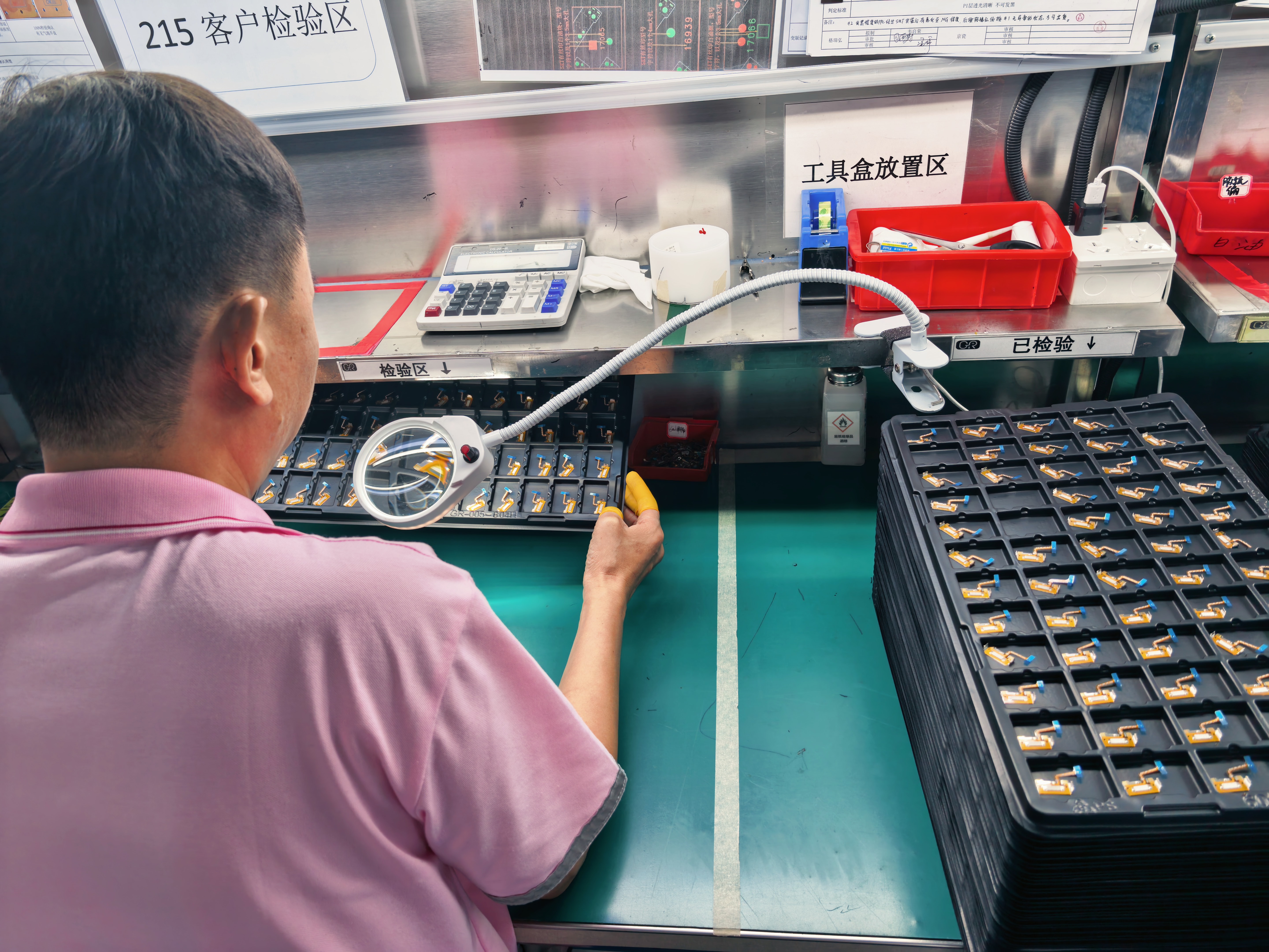
Rigorous Quality AssuranceEvery production panel undergoes comprehensiveAutomatic Optical Inspection (AOI), Microsection Analysis, and high-frequency TDR testing against Keysight baselines to fully eliminate trace defects, open/short circuits, or delamination.
Expand Your Mobile Hardware Portfolio
From initial high-speed layout optimization and precise stack-up architecture to turnkeyFlexible Printed Circuit BoardFabrication and precision SMT assembly deliver an ultra-clean, minimalist design that optimizes performance and simplifies your final assembly line. Partner with us to build a rugged, future-proof, and exceptionally reliable flexible electronic backbone for your next smartphone platform!